hotline:+86-0755-23762446

Server hardware architecture providerFocus on server hardware sales and various storage customization services
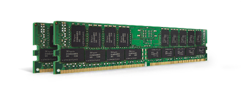
HMA82GR7CJR8N


Power Supply: VDD=1.2V (1.14V to 1.26V)
• VDDQ = 1.2V (1.14V to 1.26V)
• VPP - 2.5V (2.375V to 2.75V)
• VDDSPD=2.25V to 2.75V
• Functionality and operations comply with the DDR4 SDRAM datasheet
• 16 internal banks
• Bank Grouping is applied, and CAS to CAS latency (tCCD_L, tCCD_S) for the banks in the same or different bank group accesses are available
• Data transfer rates: PC4-3200, PC4-2933, 2666, PC4-2400, PC4-2133, PC4-1866, PC4-1600
• Bi-Directional Differential Data Strobe
• 8 bit pre-fetch
• Burst Length (BL) switch on-the-fly BL8 or BC4(Burst Chop)
• Supports ECC error correction and detection
• On-Die Termination (ODT)
• Temperature sensor with integrated SPD
• This product is in compliance with the RoHS directive.
• Per DRAM Addressability is supported
• Internal Vref DQ level generation is available
• Write CRC is supported at all speed grades
• DBI (Data Bus Inversion) is supported(x8)
• CA parity (Command/Address Parity) mode is supported
- Previous: HMCG98BDJHA464N DDR5 96G 2RX4 8800 RDIMM
- Next: HMA82GR7CJR4N


